RESEARCH
Why is everything wrapped in aluminum foil??
Chamber 1 -Selective Atomic Layer Deposition and Low Temperature-STM
Operated by: Jing and James
The system consisted of a load-lock chamber, a deposition chamber, and an ultra-high vacuum (UHV) chamber for loading samples, deposition, and XPS analysis, respectively. The load lock chamber facilitates sample transferring without breaking the vacuum of the deposition and UHV chamber. The deposition chamber has a base pressure of approximately 1×10^(−6) Torr, achieved by a turbo pump backed by a rotatory pump. The dosing lines are positioned 3 inches above the sample stage which is equipped with a cartridge heater. Currently we are working on depositing low k materials.
Chamber 2 - Variable Temperature-STM/AFM with KPFM
The cluster tool includes two ALD chambers and one in-situ XPS for chemical composition analysis. Recently, we focus on the restoration of Cu grain and highly selective Co ALD. Cleaning chamber is also equipped with Ar and N2 plasma which can do cleaning and passivation afterwards.
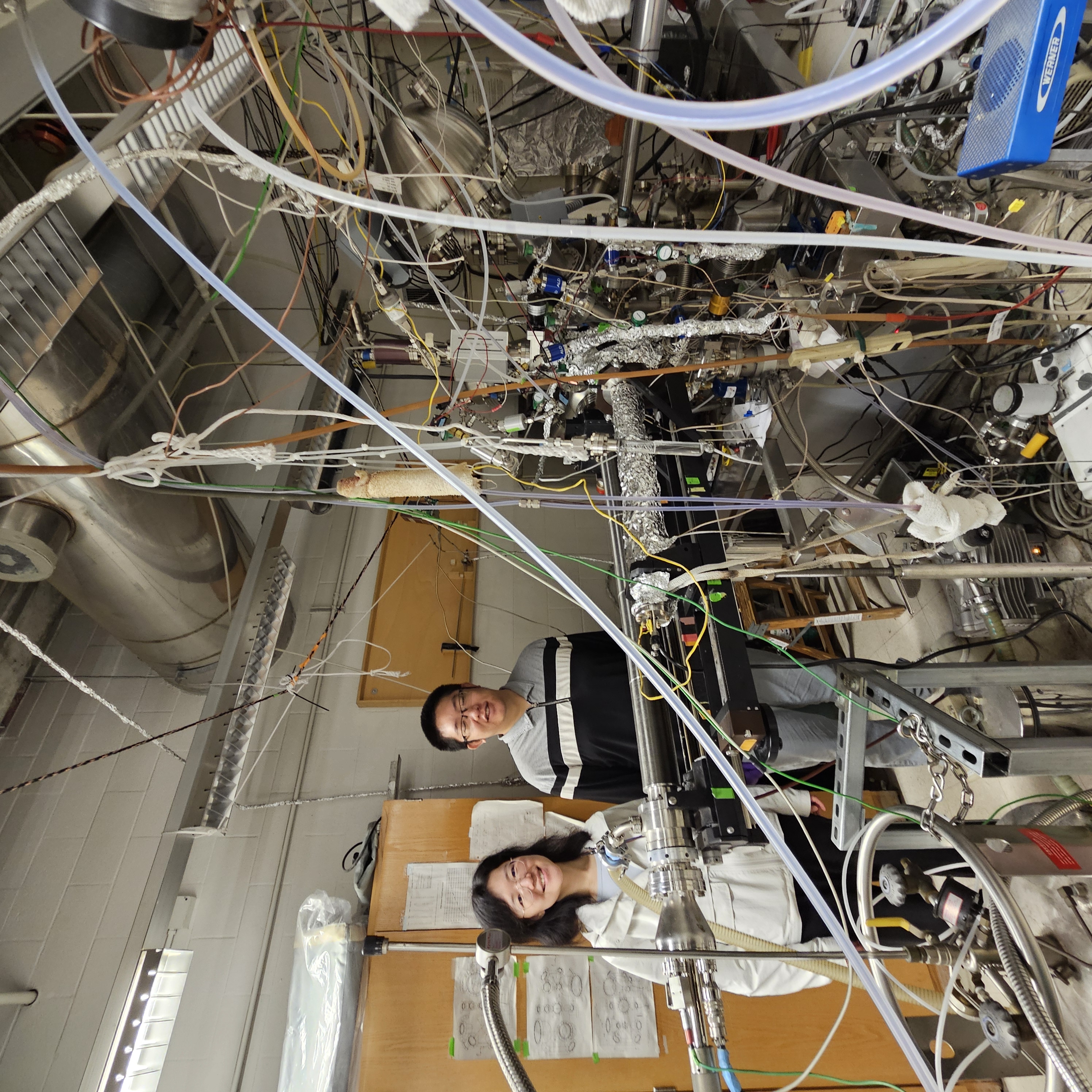
Chamber 3 - Variable Temperature-STM/AFM with KPFM and XPS
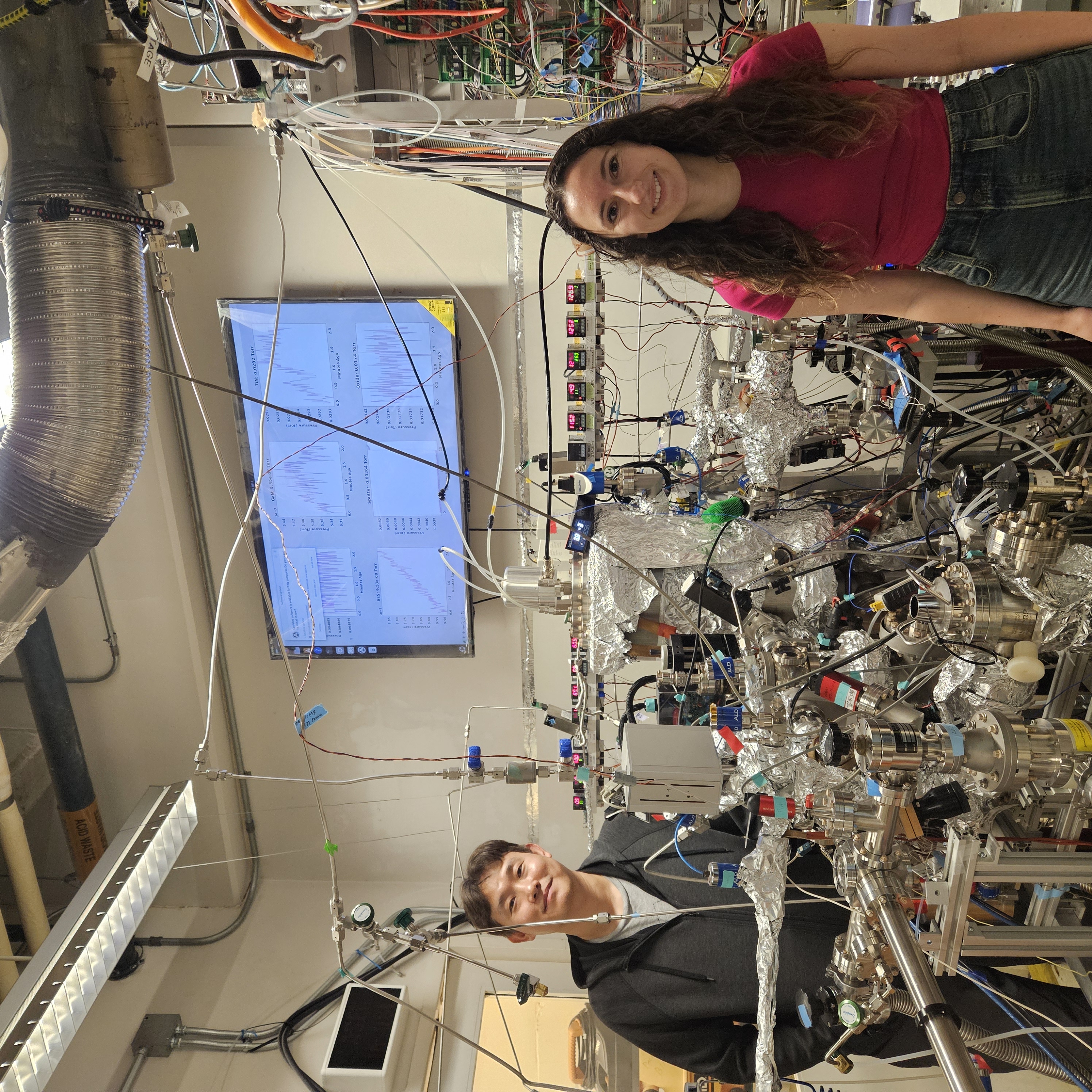
This home-built system is composed of four vacuum chambers and manipulator systems for sample transfer without vacuum break: a load lock, an atomic layer deposition system with plasma source, a sputtering chamber with DC, RF, and HiPIMS power supplies, and an analytical chamber with Auger, XPS, mass spectrometry and low-temperature scanning tunneling microscopy capabilities. Currently, the ALD chamber is being used to develop atomic layer annealing (ALA) techniques for the deposition of crystalline group III-nitride materials at low temperature (<400 ˚C). We combine this process with precursors suited for low-temperature deposition: tris(dimethylamido) aluminum and gallium complexes paired with anhydrous hydrazine. This deposition system is unique in having the ability to apply a DC or RF substrate bias, such that the kinetic energy of the bombarding ions in ALA can be controlled independently of ion flux. This allows for optimization of the surface adatom mobility, which enables the deposition of crystalline materials. Further, the periodic ion bombardment employed in ALA removes residual ligands from the growth surface, leading to deposition of nearly contaminant-free films: typical oxygen and carbon content is <2.0 at.% by XPS. The sputtering chamber is currently being used for bipolar high power impulse magnetron sputtering (HiPIMS) of aluminum nitride for the deposition of films with high thermal conductivity. These two deposition techniques can be combined to first deposit a highly crystalline template layer by ALA on a non-lattice matched or insulating substrate, which then enhances the crystallinity of material sputtered onto the template layer. Such stacked structures have demonstrated greater thermal conductivities relative to purely sputtered films of equivalent thickness. All of these films can be characterized by Auger electron spectroscopy and/or x-ray photoelectron spectroscopy to quantify film composition and trace impurities. Chamber 4 - Cluster tool with nitride/phosphide/oxide chamber and AES
Amy is studying the synthesis of titanium nitride using thermal ALD in high aspect ratio spaces. SeongUk is fabricating the the high-k material HZO using oxide chamber. He is also working on low temperature deposition of crystalline AIP and GaP on semiconductors using several ALD techniques; thermal ALD, electron enhanced ALD, atomic layer annealing, and plasma enhanced ALD. Research Poster Last updated: 03/25/2020
Operated by: Jimmy, Hyeokin, and Jit
Operated by: Ping-Che and Diego

Operated by: SeongUk and Amy